Figure 1
8 MB Memory for your Palm III
Background
People have been upgrading palm devices for some time now. With the help of Steve's Pilot Tech. Page, many people upgraded their pilot 1000/5000, and palm pilot personal/professionals to 512k, 1M or 2M. These upgrades took advantage of the way that the memory modules were constructed. Even though the palm pilot series was not available with a 2M configuration from the manufacturer, the memory module had built in support for 2M. All that was needed was to add more memory chips to the available space. Unlike the Pilot and Palm Pilot devices, the Palm III memory modules already came with 2M of memory. There was no empty sockets to fill. However, Till Harbaum figured out a way to 'stack' more chips on the card, effectively doubling the capacity of the Palm III devices to 4M. This upgrade was much more difficult to apply. He published details on his web page, and the daring ones who applied the upgrade successfully were well rewarded! [His upgrade can also be applied to the Palm III upgrade chips that 3COM manufacturers that are used to upgrade a palm pilot to 2M with OS3 and infrared support -- although the modules look different than the Palm III modules, they have the same components on them]
More recent Palm III devices were manufactured with an entirely different memory module in them. Instead of 4 SRAM chips (each providing 512k memory), these new modules had a single 2MB DRAM chip. DRAM chips are also manufactured with an 8MB capacity, in a chip that has the same physical dimensions as the 2MB chip (there is also a 16MB chip in early availablity now). On March 5, 1999, I successfully determined how to swap the existing 2MB chip with an 8MB chip and quadruple the capacity of a Palm III!
|
Figure 1 |
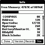
Like Till's 4M upgrade, this one requires 'advanced' soldering skills. The memory chip has even closer pins than the pins on the SRAM chips that were used in all of the previous upgrades mentioned above. The good news is that we only need to worry about 1 new chip instead of 4. The larger capacity chip will cause your device to draw more power. In my case, I could only find a replacement chip that was rated for higher speed than required, which draws even more power. If you're like me, the prospect of 8MB (see image at left) makes the battery changes tolerable. |
How it works
The simple answer is that we added more memory. The messy part is getting the memory to 'respond' to the right memory access requests.
| There was a fair bit of work involved figuring out exactly how to go
about this upgrade. The first step was to compare the operation of the
new 8M DRAM to the original 2M DRAM.
The DRAM memory on the original board is a 16Mbit (2MByte) chip. It has 44 pins. The replacement DRAM is a 64Mbit (8MByte) 50 pin chip. The chips have the same dimensions. However, the smaller chip is 'missing' some pins at the middle section of the chip (3 on each side), as illustrated at the left. Notice that while many pins on both chips are identical, there is a handful which are in different locations. This means that we can not simply solder the new chip in the place of the old one! |
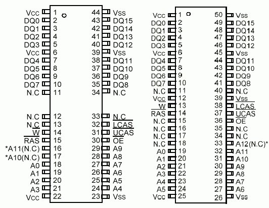
figure 2: DRAM chips. 2Meg on the left, 8Meg on the right. |
Understanding DRAM memory access.
Each location in a DRAM memory chip provides 1 word (2 bytes) of data per address. Each address is one cell in a huge array of memory, and is identified by ROW and COLUMN address. The DRAM chip can only 'read' either a row address or a column address. It does not read both at the same time. Since the CPU requests data from memory using a single address, an interface between the CPU and the memory is required. This is a DRAM controller that works in conjunction with a multiplexor. Together, they translate the single large address into two smaller (row and column) addresses, and provide them to the DRAM one at a time. The multiplexor acts as a huge gang switch which is flipped back and forth by the controller. It has 2 sets of 12 inputs, and one set of 12 outputs. The outputs (at the pins A1 to A12) are copies of either the '1B' inputs (1B1 to 1B12) or the '2B' inputs (2B1 to 2B12). Confused yet?
| You may ask why the multiplexor details are relevant. Unfortunately,
it is a necessary evil. We will need to integrate 2 new address lines into
the arrangement to take advantage of the added memory on the new chip.
The original 2M DRAM accesses memory using 8 address lines to identify
the row, and 12 for the column. The 8M DRAM will use 10 lines for the row,
and 12 for the column. Determining where to add these two new lines is
not straightforward.
In the diagram at the right, the information inside the box represents the pinout diagram of the multiplexor (a Texas Instruments SN74ALVCH16271 "12-bit to 24-bit multiplexed bus exchanger with 3-state outputs"). Outside the box, I have listed what each of the 24 input and 12 output pins is connected to. 'cAx' means the connection is to an address present on the connector strip of the memory module (and hence the CPU). '2mAx' indicates an address line of a 2M DRAM chip. '8mAx' indicates an address line of an 8M DRAM chip. [It is necessary to distinguish the 2M vs 8M address labels since the same name (eg: A0) represents a pin that is at a different physical location on the two packages (see figure 1)] We can see that all CPU address lines from cA1-cA20 are used, and that the 2M DRAM address lines 2mA0-2mA11 are used. We now need to map out exactly which CPU address lines 'appear' at the DRAM for each of the two states the multiplexor can be in. Only after this is done can we determine how to add the two new lines. [Note that only 20 address lines (not 21) are needed to access the full 2MB since 2 bytes are extracted for each address. Likewise, only 22 are needed to access 8MB.] |
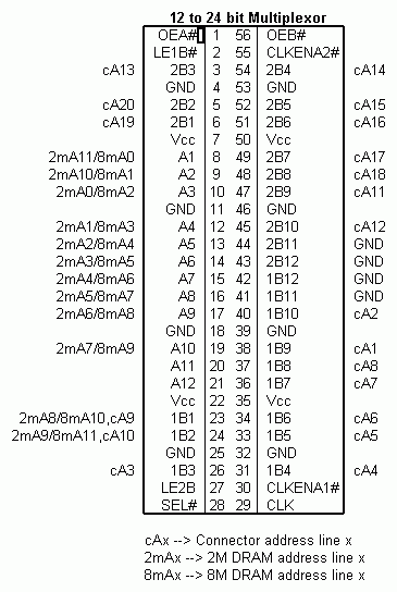
Figure 3: Multiplexor pinout and connections |
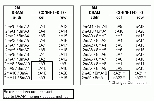
figure 4: Impact of multiplexor on address lines 'visible' to DRAM chip |
Armed with the knowledge in figure 2, it is now possible to map out
exactly which address lines from the connector strip are presented to the
DRAM chip for each of the row and column address.
For both the 2M and 8M chip, 12 address lines are used to represent the 'row'. For the 2MB chip, only the first 8 lines are used to represent the column, while the 8MB chip uses the first 10. We're very lucky that all of cA1-cA10 end up associated with 8mA0-8mA9. This means that no changes are required to access the DRAM column address properly. Also, cA11-cA20 end up associated with 8mA0-8mA9 in the row configuration, so they are fine. The only change we need then is to associate 8mA10/8mA11 with cA21/cA22 in the row configuration. Again we're very lucky, since we can avoid changes at the multiplexor, since having cA21/cA22 present when the DRAM is reading a column address won't matter -- those addresses are ignored at that time! So, if we change pins 2mA8/8mA10 and 2mA9/8mA11 to connect to the address lines at the connector cA21/cA22, then the 8M chip will use A1-A10 as its column, and A11-A22 as its row. Whew! It's hard to believe that such a simple change will work in such a complicated arrangement. |
ENOUGH ALREADY! Where are the details??
Right here!
WARNING
(All of this should be obvious, but I'm saying it anyway)
|
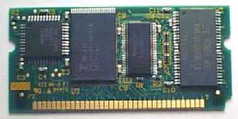
Figure 5: The PIII 2M board |
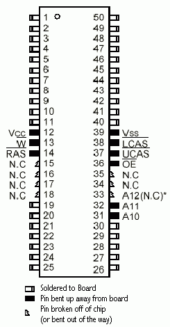
Figure 6: DRAM preparation |
|
Now there are 5 connections that must be made to pins that were present on the original chip, but are in different locations on the new chip. It is possible to use very fine wire, and just create use very small lengths of it to make each of these connections from the new pin to the old pad. I do NOT recommend this (I didn't even do it). However, the appropriate connections would be: Instead of those five connections, it is possible to use longer lengths of wire and connect to pins on the small square chip at the left of the board. Using the longer lengths of wire provides something to hold on to while soldering, and also means that there is less solder work near the new chip (which would otherwise be very cluttered with new solder connections). The following five connections will all refer to connections between the DRAM memory chip and the small square chip at the left (which I will refer to as the controller chip). Up/down/left/right assume that you have the connector strip on the bottom, as in the illustrations at the right. The final two connections are for the extra two address lines. The gold connector strip along the bottom is numbered. The side all of the components is mounted on has all the even connectors (numbered from right to left). The odd connectors are on the back of the board. We must connect directly to these connectors. Be careful to leave most of the connector free of solder as this would reduce the quality of the connection. |
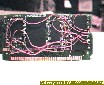
Figure 7 (Very messy, but it was a prototype!) 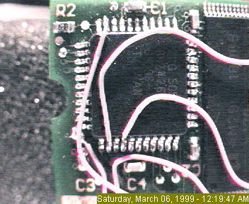
Figure 8 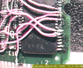
Figure 9 (I hope your soldering is better than mine was. Yuch.) |
That's it!
| Check all your work for accidental shorts. Be especially careful at the extreme right edge of the board. There are four connections very close to the hold-down cutout on the board. If your solder joints extend too far right, these will be damaged when you insert the board. Ensure that all wires are safely tucked away, and are clear of the connector strip and hold-downs on the sides. Carefully insert the board. Insert the batteries, and do a reset. If all is well, you'll have quadrupled the capacity of your favorite PDA! | |
PARTS
I have already received a few requests from people looking for the replacement DRAM part number. The new part must be a 64Mb DRAM chip, Low power (3.3v), have a 4k refresh, and be rated at 60ns or better (lower). The old chip as well as the new chip I used were both Fast Page Mode chips. Theses are getting hard to find (especially in small quantities). It is also possible to use an EDO chip, which is pin compatible with the FPM chip. (Note that while EDO performs better than FPM, it won't be any faster in this application since the board wasn't created to take advantage of EDO features).
The part I removed was a Samsung KM416V1000BT-L6. The Samsung 64Mb part number is KM416V4100. (The suffix would have A,B,C depending on generation, then T for the TSOP package style, "-L" for low power, and a -45, -5 or -6 representing either 45, 50, or 60ns speed). The "-L" is not required. You can also use a KM416V4104 chip. I actually used a MICRON MT4LC4M16F5TG-5 chip (MT4LC4M16R5TG-6 works too). Hyundai makes the HY51V65160A series (I don't know the suffix required -- look for a low power tsop chip). NEC makes the uPD4265165 (uPD42S65165).
If you have an interest in doing this upgrade yourself, but can not find any chips, then contact me. I have single chips available for sale at a cost of $30 USD each. These chips are suitable for the upgrade described here. If you need a chip for the Palm V upgrade (described elsewhere), contact me to see if I have any that are compatible.
Parts Links
Upgrade Service
If you would like to have me perform this upgrade on your unit, check out my Upgrade Service page.
Palm Links
Check out my other palm pages at http://www.ImpressiveStuff.com.